Cellular Interfaces
Compressive buckling for three-dimensional transistor arrays
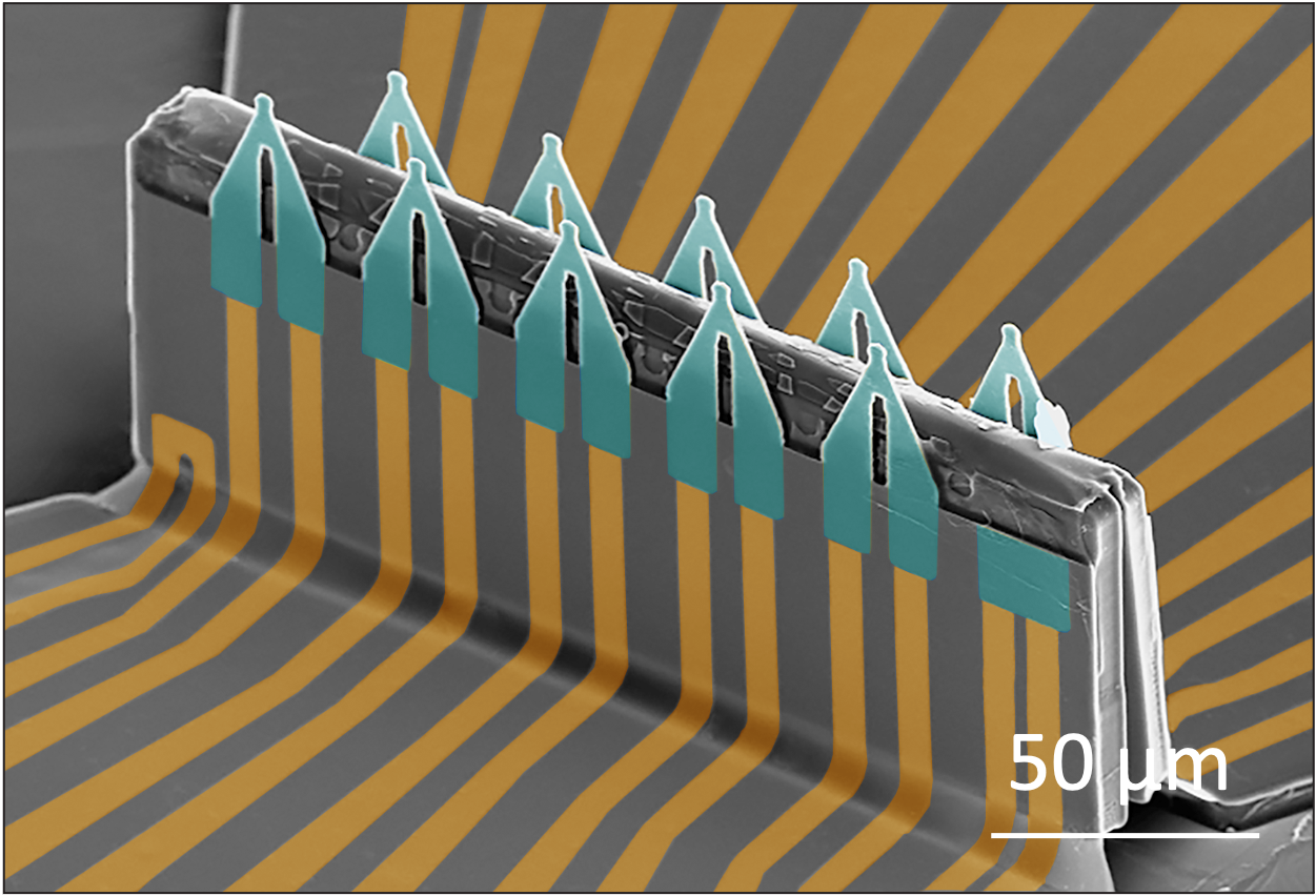
Compressive buckling is a novel fabrication technology to build designed complex 3D micro/nanostructures via the out-of-plane buckling of a corresponding planar precursor layout. The 3D buckling method features high throughput with rapid and large scale fabrication, versatility in material selection (metals, ceramics, and polymers in crystalline or amorphous forms), and potential to build soft electronic devices. We used compressive buckling to build an array of three-dimensional field effect transistors based on device-grade silicone. Those transistors have a tip size of ~ 1 µm, high sensitivity, low noise, different heights, and most importantly, a short response time of ~ 700 µs, which allowed them to pick up various cellular signals.
Intra- and inter-cellular recording of cardiomyocytes
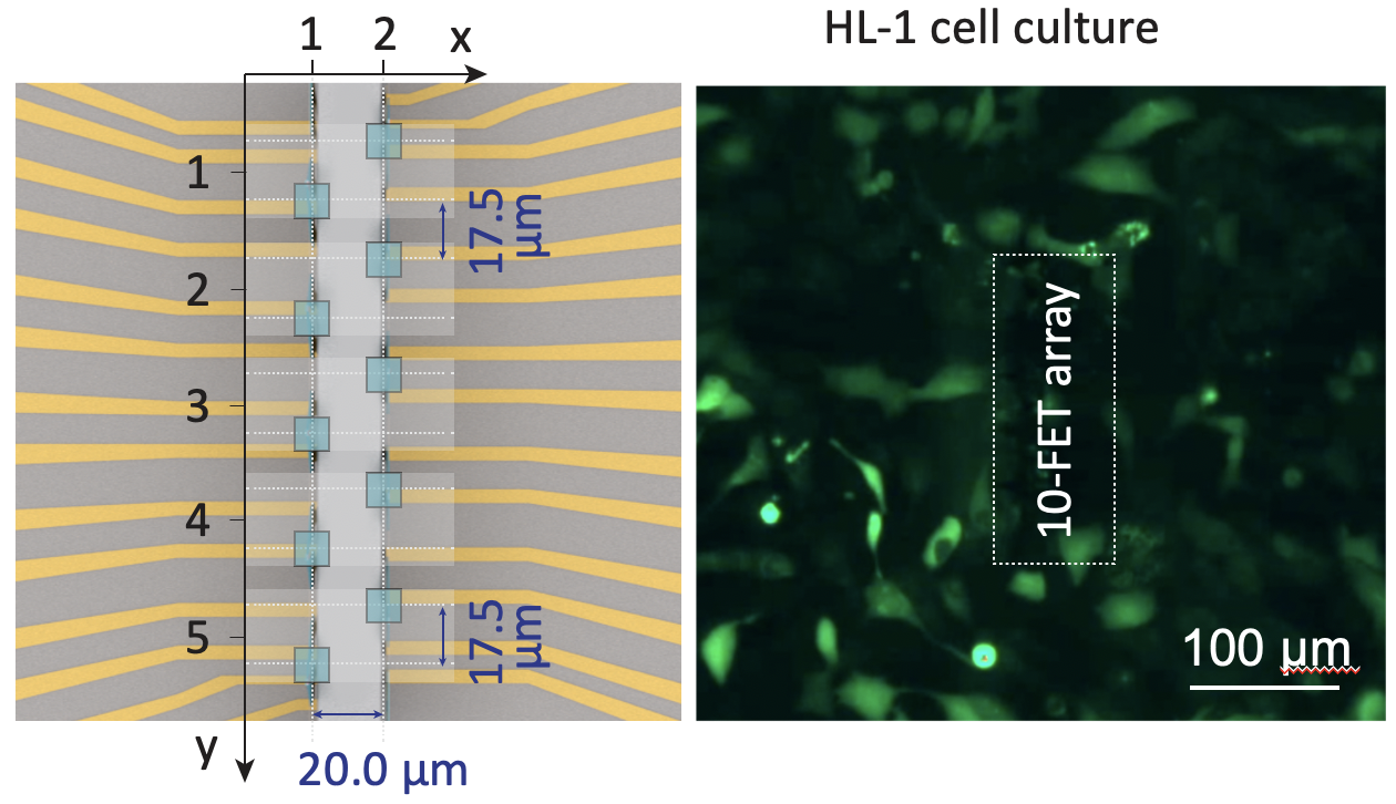
Electrical communications between cells serve as the basis for electrophysiology. We applied the three-dimensional transistor arrays to study the electrical communications in cardiomyocytes of two-dimensional culture and three-dimensional organoid. With well-defined spacing between the transistors, recording the signal latency among different transistors allows inferring the directions and calculating the velocities of signal conduction. Particularly, when the transistor spacing is smaller than the cell size, we were able to insert two transistors inside one cell, which enables direct recording of signal conduction inside the cell. The recorded intracellular conduction velocity is about six times the velocity of intercellular velocity measured conventionally.

